
[ad_1]
Mar 17, 2024
(Nanowerk Highlight) For brand new era digital home equipment superior nanoscale transistors are in demand which wants exact biasing of every system. These stringent biasing circumstances may be relaxed by acquiring exact values of the edge voltages of the transistor. This will even enhance tolerance of digital logic states to electrical noise. The necessities of lowered energy consumption are achieved in CMOS field-effect transistors (FETs) by fabricating and working it in enhancement (E) mode i.e. absence of free cost carriers within the channel at zero gate voltage.
To make clear, within the context of field-effect transistors, enhancement mode (E-mode) refers back to the state the place the system requires a sure gate voltage to induce a conducting channel between the supply and drain terminals. Conversely, depletion mode (D-mode) FETs inherently have a conducting channel at zero gate voltage, requiring a gate voltage of reverse polarity to ‘deplete’ or flip off the channel. This basic distinction performs an important position in how units are designed for particular purposes, impacting their energy consumption, pace, and total performance.
However, depletion (D) mode transistors have greater currents than enhancement mode on account of ample cost provider density. In distinction to switching utility of FET, for high-frequency purposes off-state of FET isn’t a obligatory requirement. In reality, the presence of a channel at zero gate bias is advantageous to acquire excessive transconductance at decrease voltages. For Si FETs, the enhancement or depletion modes had been decided on the fabrication step of ion implantation doping. Nonetheless, it’s difficult to implement this answer for the brand new era of skinny supplies like natural semiconductors and 2D supplies.
In response to new analysis printed within the journal of ACS Utilized Digital Supplies (“Selective Operation of Enhancement and Depletion Modes of Nanoscale Subject-Impact Transistors”), by selecting a specific work perform for a gate steel, threshold voltages of the p-type FETs may be modified from unfavorable to constructive values that’s selective switching between enhancement mode to depletion mode of the operation.
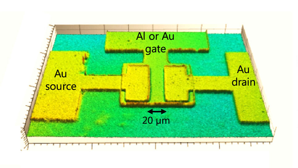
3D optical profiler picture of the fabricated FETs. (Reprinted with permission by American Chemical Society)
The researchers experimentally fabricated the FETs with numerous gate steel electrodes having completely different work capabilities. The dielectric alumina thickness was simply 5 nm. Because of this brief separation between gate steel and natural p-type semiconducting channel, there’s electrostatic interplay between them even with out the applying of exterior voltage. When low-work perform steel like aluminum (4.4 eV) is used, the FET operates in E-mode. For top-work perform gate metals like gold (5.0 eV), a sure variety of holes are induced within the channel at zero gate voltage. This results in a superb quantity of present within the channel which is named D-mode operation.
Complementing their groundbreaking experimental efforts, the analysis crew employed superior TCAD system simulations, which had been instrumental in validating their findings. These simulations, producing colour contour plots of induced gap density, supplied each a visible and theoretical verification of the affect of gate steel work capabilities on the FETs’ operational modes. This complete strategy, marrying experimental information with simulation insights, not solely enhances the credibility of the analysis but in addition emphasizes its significance for technological developments and potential for scale-up in manufacturing.
The lead creator Dr Abhay Sagade from SRMIST, India, revealed that the noticed results are profound for skinny dielectric thickness comparable to lower than 10 nm. “For the bigger thicknesses, the FETs stay in enhancement mode even for top work perform gate metals,” he notes. “This idea may be simply extendable to any skinny natural, inorganic and new era 2D supplies.”
An necessary side of this examine is the concentrate on the thickness of the dielectric layer utilized in FETs. Researchers discovered that the results noticed—switching between enhancement and depletion modes—had been pronounced for skinny dielectrics, particularly these lower than 10 nm. This discovering highlights the crucial position of dielectric thickness in influencing FET habits, emphasizing the necessity for exact management over materials properties to realize desired system efficiency.
Utilizing this technique, it must be potential to manufacture extra compact-sized correct and reconfigurable digital logic, and oscillator units and circuits. Additional, D-mode OFETs with improved currents may be utilized effectively for high-frequency purposes. This additionally has immense implications for upcoming quantum units and technological purposes which use small dimensional delicate units.
Past the instant advantages for digital logic and oscillator units, the flexibility to selectively change between operation modes holds immense promise for high-frequency purposes, doubtlessly revolutionizing the design of next-generation quantum units. The flexibility of this technique paves the way in which for modern digital parts that aren’t solely extra environment friendly and compact but in addition extremely reconfigurable, assembly the various wants of contemporary know-how landscapes.

By
Michael
Berger
– Michael is creator of three books by the Royal Society of Chemistry:
Nano-Society: Pushing the Boundaries of Expertise,
Nanotechnology: The Future is Tiny, and
Nanoengineering: The Expertise and Instruments Making Expertise Invisible
Copyright ©
Nanowerk LLC
Nanowerk E-newsletter
Get our Nanotechnology Highlight updates to your inbox!
Thanks!
You might have efficiently joined our subscriber checklist.
Change into a Highlight visitor creator! Be part of our massive and rising group of visitor contributors. Have you ever simply printed a scientific paper or produce other thrilling developments to share with the nanotechnology group? Right here is the right way to publish on nanowerk.com.
[ad_2]
Supply hyperlink

