[ad_1]
Mar 22, 2024
(Nanowerk Information) Steel halide perovskites have turn out to be well-deserved “star” supplies amongst a wide range of semiconductors owing to their wonderful optoelectronics properties, comparable to excessive photoluminescence (PL) quantum yield (QY), excessive absorption coefficient, tunable bandgaps, lengthy service diffusion lengths, and excessive defect tolerance, attracting monumental consideration from each academia and trade.
In the meantime, DLW, based mostly on the interplay between gentle and matter, is an environment friendly, contactless, masks free, and depth-resolved micro-patterning method. It’s sometimes carried out by coupling a laser beam with a high-resolution microscope to attenuate the output focal spot. The decision of DLW depends on the diameter of the output focal spot and the brink response of the fabric.
Relying on the fabrication mechanisms and materials threshold responses, one of the best decision is often between a pair to a couple a whole bunch of nanometers. The analysis on DLW additionally deepens the basic understanding on the interplay mechanisms between gentle and perovskites, paving the way in which for designing optoelectronic gadgets with improved performances.
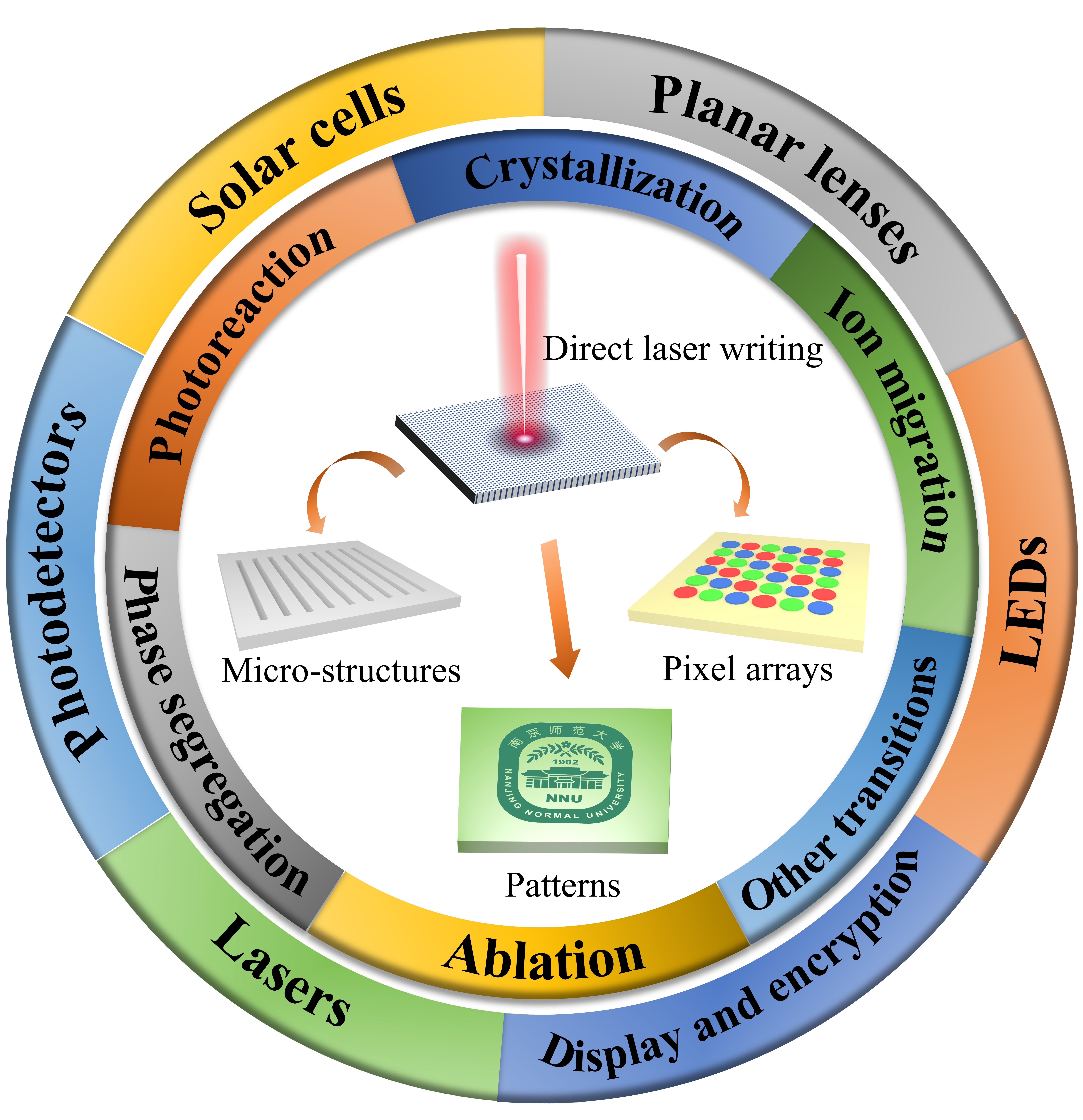
In a evaluation paper printed in Mild Superior & Manufacturing (“Direct laser writing on halide perovskites: from mechanisms to purposes”), a workforce of scientists, led by Professor Zhixing Gan from Heart for Future Optoelectronic Practical Supplies, Nanjing Regular College, China, and colleagues have summarized latest analysis progress of DLW on perovskites.
Schematic overview of direct laser writing on halide perovskites: from mechanisms to purposes. (Picture: Mild Superior & Manufacturing)
The concrete interplay mechanisms between laser and perovskite are categorized into six elements, together with laser ablation, laser induced crystallization, laser induced ion migration, laser induced part segregation, laser induced photoreaction, and different laser induced transitions. Then, they concentrate on the purposes of those perovskites with micro/nano patterns and array constructions, comparable to show, optical data encryption, photo voltaic cells, LEDs, laser, photodetectors, and planar lenses. The benefits of the patterned constructions are highlighted. Lastly, present challenges for DLW on perovskites are outlooked and views on their future developments are additionally put ahead.
Laser is a superb device to govern, fabricate and course of nano-/micro-structures on semiconductors with distinctive benefits of excessive precision, contactless, straightforward operation, masks free. DLW based mostly on completely different interplay mechanisms between laser and perovskites have been developed as a result of particular construction of perovskites. The detailed interplay mechanism sensitively is dependent upon laser, comparable to wavelength, pulse/CW, energy, and repetition fee, subsequently offering a versatile and highly effective device to course of the perovskites with exactly managed nano- or micro-structures. The wide range of interplay mechanisms decide the DLW’s nice potential for numerous purposes in microelectronics, photonics and optoelectronics.
Cheaper and flexibly controllable fabrication lasers, along with perovskite’s superior optoelectronic properties will convey nice software potential for DLW on perovskites. Presently it’s nonetheless within the infancy stage, anticipating an enormous growth in each elementary analysis and trade demand within the close to future. For the long run improvement of DLW on perovskites, some essential technical bottlenecks must be solved, such because the decision of DLW method, the prevailing time of segregated phases, and the micropatterning method to versatile substrates, and many others.
The purposes of perovskites nearly cowl all kinds of optoelectronic and photonic areas, comparable to single photon supply, micro/nano lasers, photo-detectors, optical gates, optical communication, waveguide, and nonlinear optics. Thus, it is vitally promising to assemble and combine photonic gadgets with completely different capabilities based mostly on a single perovskite chip.
[ad_2]
Supply hyperlink

